A316-HF-I2S-V1 USB TO I2S HiFi Audio Converter Evaluation Board Datasheet × Phaten Cloud Login/Register Login Register
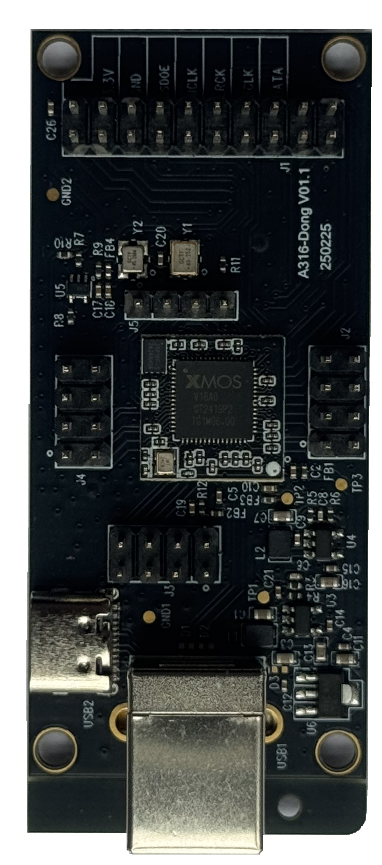
1. Product Introduction 1.1 Product Description A316-HF-I2S-V1 is designed based on the A316-Mini--V1 XU316 module, with DAC removed , focusing on USB digital signal reception and conversion A316-HF-I2S-V1 receives 2-channel USB input, decodes it, and outputs via I2S All XU316 pins are exposed on the evaluation board, allowing users to perform various development and debugging tasks for XU316 based on this evaluation board A316-HF-I2S-V1 features 2 built-in low phase noise 45.1584MHz/49.152MHz active crystal oscillators Combined with different DACs, users can use this evaluation board for various USB HiFi application evaluations, suitable for audio equipment developers and Hi-Fi DIY enthusiasts to build high-fidelity audio decoding systems 1.2 Product Features USB Interface Features USB 2.0 (Full-speed and High-speed) USB Audio Class 1.0 USB Audio Class 2.0 USB Firmware Upgrade (DFU) 1.3 Specification Description Specification Item Description Product Name A316-HF-I2S-V1 Product Description USB TO I2S HiFi Audio Converter Evaluation Board Datasheet Core Chip XMOS XU316-1024-QF60B-C24 Clock 48.152MHz/49.152MHz active crystal oscillator clock Package Type Pin header Environmental Compliance All hardware components fully comply with EU RoHS directive
1.4 Absolute Maximum Ratings Parameter Minimum Maximum Unit Storage Temperature -40 125 ℃ Supply Voltage -0.5 5.63 V Electrostatic Discharge Voltage (Human Body Model) TAMB-25℃ -2 2 KV Electrostatic Discharge Voltage (Machine Model) TAMB-25℃ -500 500 V
1.5 Normal Operating Conditions Function Minimum Typical Maximum Unit Operating Temperature 0 - 70 ℃ Operating Voltage 4.95 5.0 5.63 V
1.6 Operating Current Operating Status Average Peak Unit Active@5V 90 150 mA
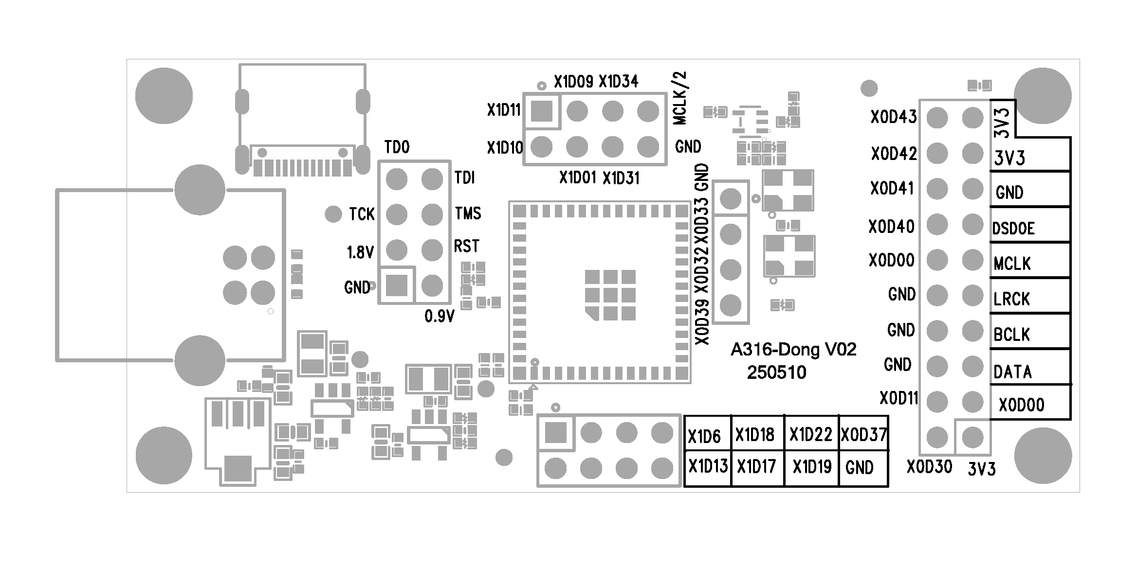
2. Pin Definition 2.1 Pin Layout 2.2 Pin Description Audio Output Interface No. Name Type Function 1 3.3V P Outputs 3.3V high level when USB cable is inserted 2 XOD00 I/O I2C CLK 3 DATA I/O I2S (Master) DATA 4 BCLK I/O I2S (Master) BCLK 5 LRCK I/O I2S (Master) LRCK 6 MCLK I/O I2S (Master) MCLK, 49.152MHz or 45.1584MHz 7 DSDOE I/O Outputs 3.3V high level when DSD stream is detected 8 GND P Ground 9 3V3 P 3.3V power output 10 3V3 P 3.3V power output 11 XOD30 I/O DAC MUTE, outputs high level during sample rate change or DSD mode change 12 X0D11 I/O I2C DATA 13 GND P Ground 14 GND P Ground 15 GND P Ground 16 X1D00 I/O Multi-function GPIO 17 X0D40 I/O Multi-function GPIO 18 X0D41 I/O Multi-function GPIO 19 X0D42 I/O Multi-function GPIO 20 X0D43 I/O Multi-function GPIO
Expansion Interface 1 No. Name Type Function 1 X1D16 I/O Multi-function GPIO 2 X1D18 I/O Multi-function GPIO 3 X1D22 I/O Multi-function GPIO 4 X0D37 I/O Multi-function GPIO 5 X1D13 I/O Multi-function GPIO 6 X1D17 I/O Multi-function GPIO 7 X1D19 I/O Multi-function GPIO 8 GND P Ground
Expansion Interface 2 No. Name Type Function 1 X1D11 I/O Module clock divided output 2 X1D09 I/O Module clock divided output 3 X1D34 I/O Module clock divided output 4 MCLK/2 I/O MCLK/2 24.576MHz or 22.5792MHz 5 X1D10 I/O Module clock divided output 6 X1D01 I/O Module clock divided output 7 X0D31 I/O Module clock divided output 4 GND P Ground
Expansion Interface 3 No. Name Type Function 1 GND P Module ground 2 X0D33 I/O Multi-function GPIO 3 X0D32 I/O Multi-function GPIO 4 X0D39 I/O Multi-function GPIO
DEBUG Interface No. Name Type Function 1 GND P Module ground 2 1.8V P 1.8V power 3 TCK I Test clock 4 TDO I/O Test data output 5 0.9V P 0.9V power 6 RST I Reset signal 7 TMS I/O Test mode select 8 TDI I/O Test data input
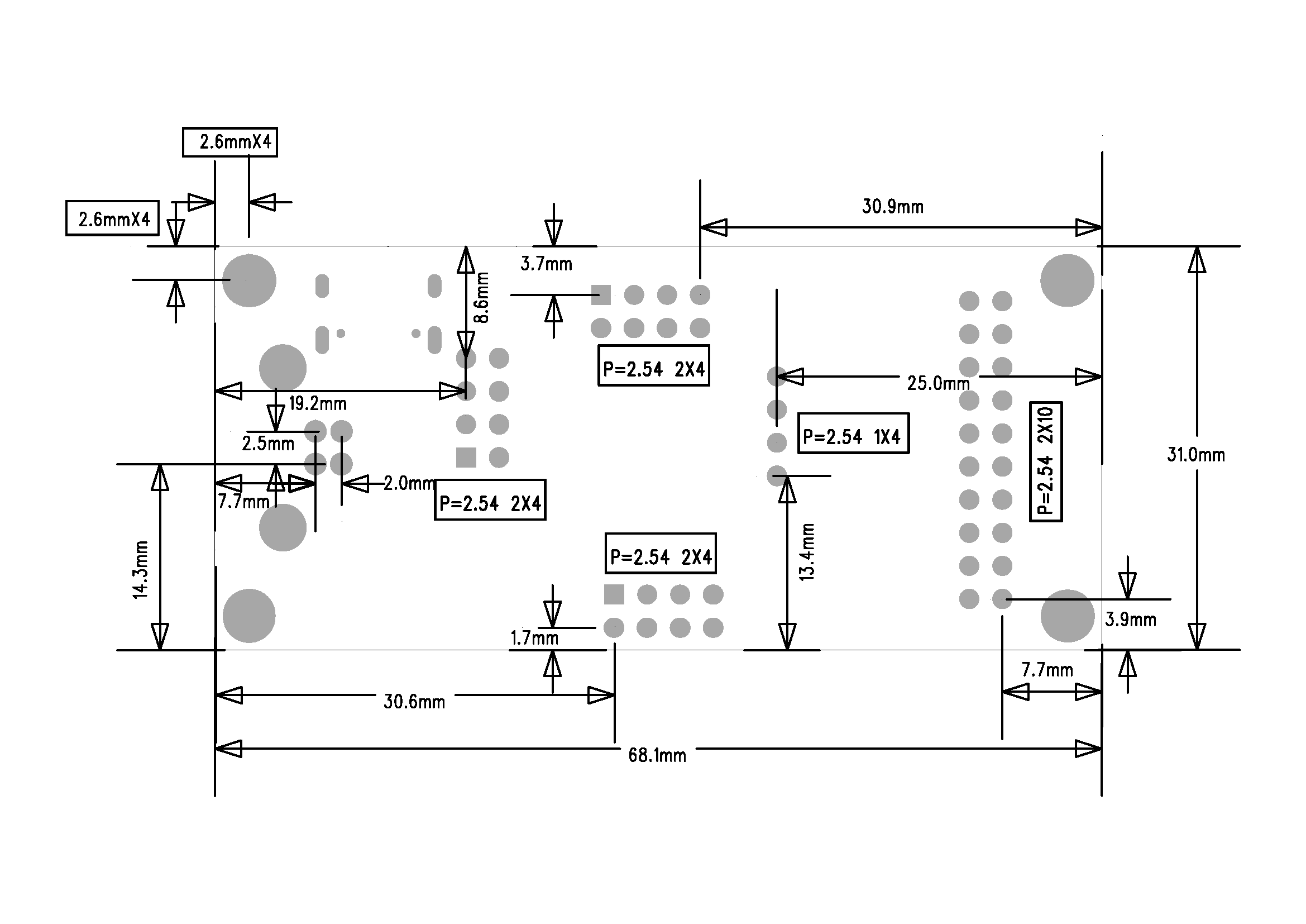
3.1 Module Dimensions PCB Dimensions: 68±0.3(L)X31±0.3(W)X1.6±0.1(H)
Tray + outer box packaging
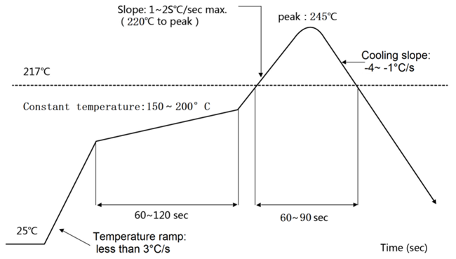
5. Recommended Reflow Soldering Temperature Profile 6. Revision History Version Date Description Revised By V1.0 2025-05-07 Initial version released
Inquiries and Feedback Click to expand inquiry and feedback form 


