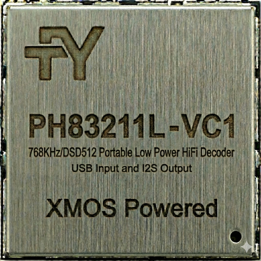
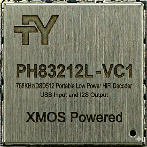
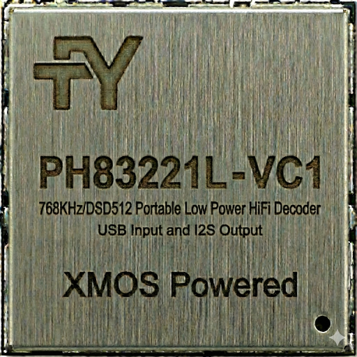
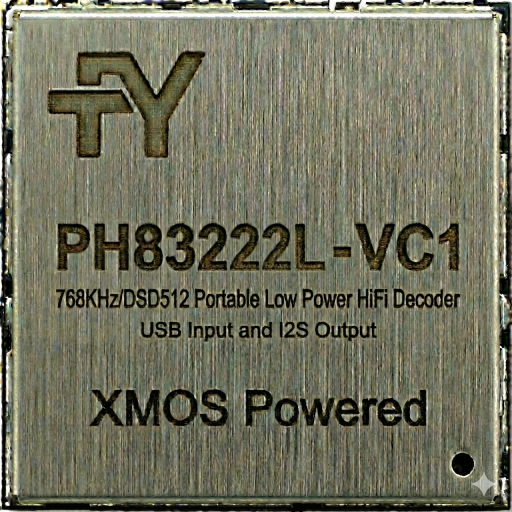
PH832XXL-VC1 Product Specifications
768KHz/DSD512 HiFi Portable Decoder with Low-Power XU316 and ES903XQ2M / CS43198/CS43131
1. Introduction
1.1 Product Description
The PH832XXL-VC1 is a USB low-power HiFi audio decoder supporting up to PCM 768KHz/DSD512, designed specifically for portable HiFi decoder audio applications. The module's firmware has been adapted and optimized for several high-performance audio DACs commonly used in portable decoders.
The PH83211L-VC1 supports multiple standard audio formats, including USB Audio Class 1.0/2.0 and I²S interface. The flexible audio interface allows the PH83211L-VC1 to connect to various audio data converters, digital audio receivers and transmitters, and digital signal processors.
XU316 Low-Power Test Comparison Results
| Chip Type | DSD 512 | PCM 768KHz | PCM 384KHz | PCM 192KHz |
|---|---|---|---|---|
| Low-Power Chip | 113 mW | 146 mW | 128 mW | 123 mW |
| Standard Power Chip | 227 mW | 232 mW | 227 mW | 222 mW |
| Power Saved | 114 mW | 86 mW | 99 mW | 99 mW |
| Power Saved % | 50.22% | 37.07% | 43.61% | 44.59% |
1.2 Product Features
USB Interface Features
- USB2.0 high-speed compatible
- Support for UAC2.0 and UAC1.0 (mode selection via button)
- USB bus powered
Audio Format Support
-
UAC2.0
Audio Format Supported Sample Rates PCM Bit depth: 16bit, 24bit, 32bit; Sample rates: 44.1kHz, 48kHz, 88.2kHz, 96kHz, 176.4kHz, 192kHz, 352.8kHz, 384kHz, 705.6kHz, 768KHz DSD Native DSD64, DSD128, DSD256, DSD512 DOP DOP64, DOP128, DOP256 -
UAC1.0
Audio Format Supported Sample Rates PCM Bit depth: 16bit; Sample rate: 48kHz
PEQ Support
- Support for 8-band 44.1-192KHz EQ
- Support for Web and APP PEQ console
System Compatibility
- Support for Windows 10 / 11[^1], Mac OS, Android[^2], iOS[^3]
- Support for proprietary ASIO driver (UAC2.0 only), enabling ultra-low latency ASIO playback
Hardware Features
- Support for function buttons, configurable via firmware
- Support for RGB status indicator LEDs, configurable via firmware
- Support for output load mode switching
- Support for digital filter switching
1.3 Application Scenarios
- USB Low-Power HiFi Decoder (USB Portable HiFi Decoder)
1.4 Product Block Diagram
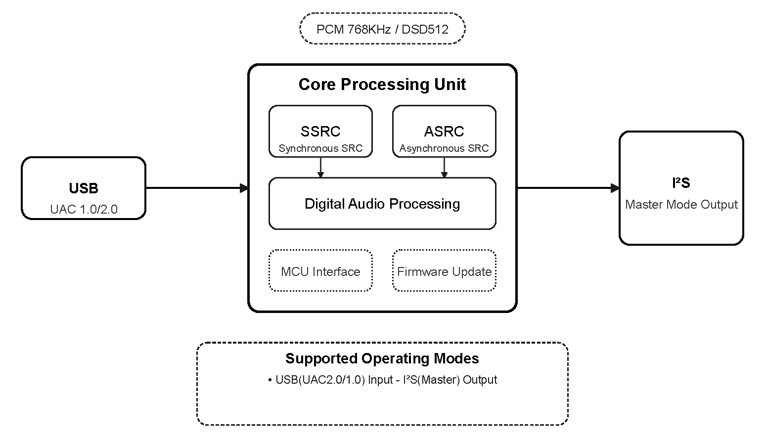
1.5 Ordering Information
2. Modes and Specifications
2.1 Supported Input/Output Modes
| Mode Number | Input/Output Mode | Description |
|---|---|---|
| 1 | USB(UAC2.0) in-I²S(Master) out | USB input, I²S output, UAC2.0 |
| 2 | USB(UAC1.0) in-I²S(Master) out | USB input, I²S output, UAC1.0 |
2.2 Detailed Parameters for Each Operating Mode
2.2.1 USB(UAC2.0) in → I²S out Mode
Supported Audio Formats and Sample Rates:
| Audio Format | Supported Sample Rates |
|---|---|
| PCM | 44.1kHz, 48kHz, 88.2kHz, 96kHz, 176.4kHz, 192kHz, 352.8kHz, 384kHz, 705.6kHz, 768KHz |
| DSD Native | DSD64, DSD128, DSD256, DSD512 |
| DOP | DOP64, DOP128, DOP256 |
2.2.2 USB(UAC1.0) in → I²S out Mode
Supported Audio Formats and Sample Rates:
| Audio Format | Supported Sample Rates |
|---|---|
| PCM | 48kHz/16bit |
3. Pin Configuration and Functions
3.1 PH83211L-VC1 Pin Layout
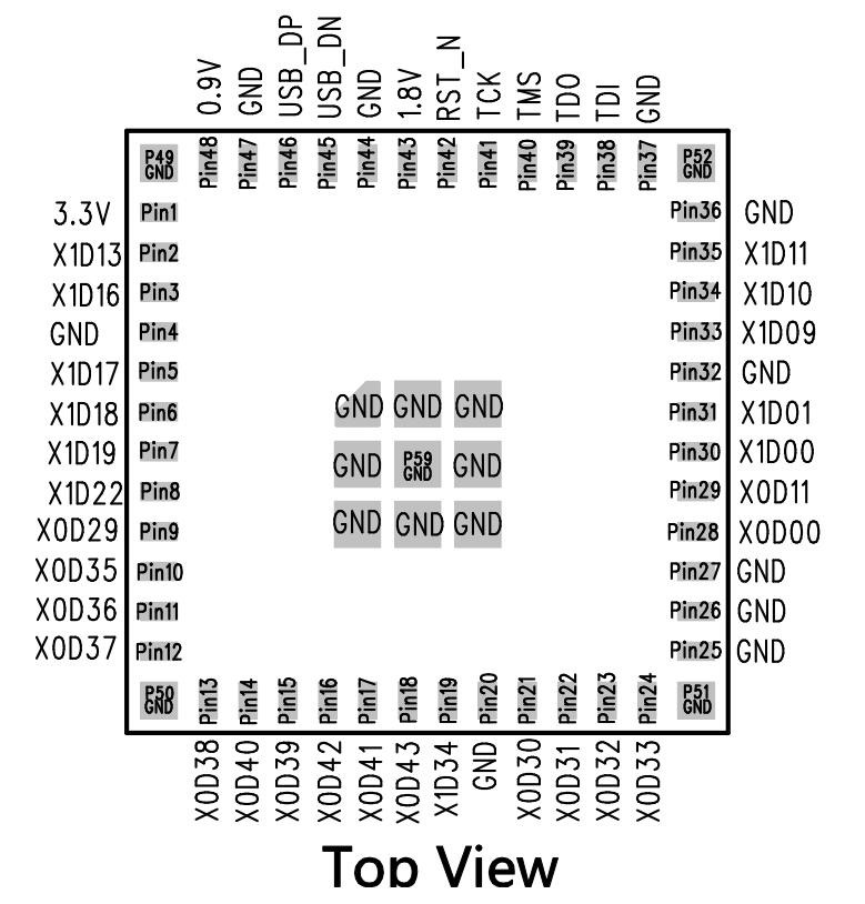
3.2 Pin Description
| Module Pin Number | Name | Type | Function Description |
|---|---|---|---|
| 1 | 3.3V | P | Module 3.3V power supply |
| 2 | X1D13 | I/O | NC (Not Connected) |
| 3 | X1D16 | I/O | NC |
| 4 | GND | P | Module ground |
| 5 | X1D17 | I/O | NC |
| 6 | X1D18 | I/O | NC |
| 7 | X1D19 | I/O | NC |
| 8 | X1D22 | I/O | NC |
| 9 | X0D29 | O | CHIP_EN: Connects to DAC's CHIP_EN pin, used to enable DAC, active high |
| 10 | X0D35 | O | I2S_BCLK: I²S bit clock, connects to DAC |
| 11 | X0D36 | O | I2S_LRCK: I²S left/right clock, connects to DAC |
| 12 | X0D37 | I | Play/MODE: Button 2: Function button, active low (supported by models PH83212L-VC1/PH83222L-VC1) |
| 13 | X0D38 | O | I2S_DOUT: I²S data output, connects to DAC |
| 14 | X0D40 | O | LED_GREEN: Drives green LED, active low |
| 15 | X0D39 | O | MCLK: Master clock output, connects to DAC |
| 16 | X0D42 | O | LED_BLUE: Drives blue LED, active low |
| 17 | X0D41 | O | LED_RED: Drives red LED, active low |
| 18 | X0D43 | I/O | AMP_POWER_EN: Headphone amplifier power enable signal, active high |
| 19 | X1D34 | I/O | NC |
| 20 | GND | P | Module ground |
| 21 | X0D30 | O | AMP_EN: Headphone amplifier enable signal, active high |
| 22 | X0D31 | O | CTRL_MUTE: Mute control signal, low level mutes, high level outputs |
| 23 | X0D32 | I | P_VOL-: Button 2: Volume down button input, active low |
| 24 | X0D33 | I | P_VOL+: Button 1: Volume up button input, active low |
| 25 | GND | P | Module ground |
| 26 | GND | P | Module ground |
| 27 | GND | P | Module ground |
| 28 | X0D00 | I/O | I2C_SDA: I²C data line, used to connect and control DAC |
| 29 | X0D11 | I/O | I2C_SCL: I²C clock line, used to connect and control DAC |
| 30 | X1D00 | I/O | NC |
| 31 | X1D01 | I/O | NC |
| 32 | GND | P | Module ground |
| 33 | X1D09 | I/O | NC |
| 34 | X1D10 | I/O | NC |
| 35 | X1D11 | O | Connected to X0D39 |
| 36 | GND | P | Module ground |
| 37 | GND | P | Module ground |
| 38 | TDI | I/O | JTAG_TDI |
| 39 | TDO | I/O | JTAG_TDO |
| 40 | TMS | I/O | JTAG_TMS |
| 41 | TCK | I/O | JTAG_TCK |
| 42 | RST_N | I | XMOS_RST |
| 43 | 1.8V | P | Module 1.8V power supply |
| 44 | GND | P | Module ground |
| 45 | USB_DM | I/O | USB D- |
| 46 | USB_DP | I/O | USB D+ |
| 47 | GND | P | Module ground |
| 48 | 0.9V | P | Module 0.9V power supply |
| 49 | GND | P | Module ground |
| 50 | GND | P | Module ground |
| 51 | GND | P | Module ground |
| 52 | GND | P | Module ground |
4. Hardware Parameters
4.1 Normal Operating Conditions
| Function | Minimum | Typical | Maximum | Unit |
|---|---|---|---|---|
| Operating Temperature | 0 | - | 70 | ℃ |
| 3.3V Operating Voltage | 3.0 | 3.3 | 3.6 | V |
| 1.8V Operating Voltage | 1.62 | 1.80 | 1.98 | V |
| 0.9V Operating Voltage | 0.855 | 0.90 | 0.945 | V |
4.2 Product Dimensions
13±0.1mm(L)X13±0.1mm(W)X0.8±0.1mm(H)
4.3 Module Package Diagram
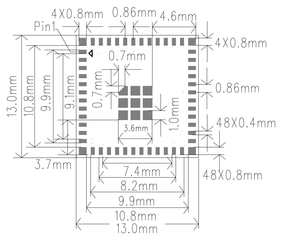
4.3 Module Schematic
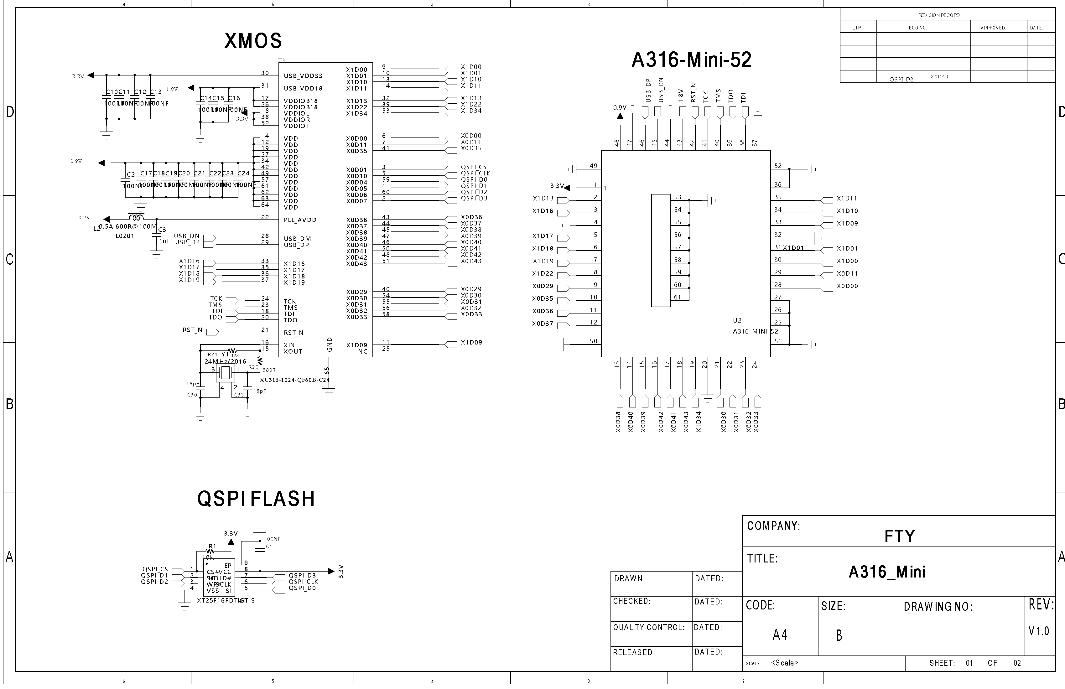
4.4 XMOS XU316 Chip Datasheet
5. Reference Design
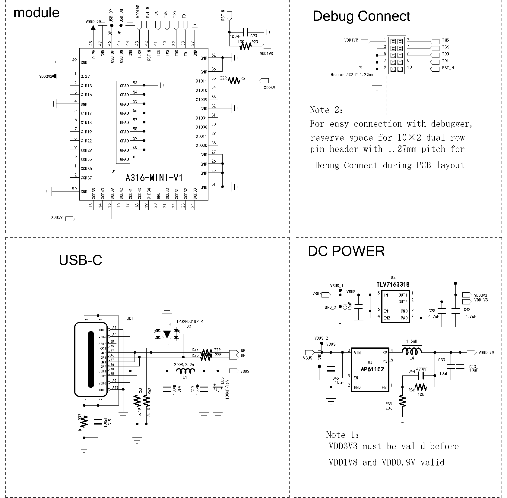
6. RGB Status Indicator LED Definitions
| UAC Mode | Audio Stream Format/Sample Rate | LED Color (Low Gain Mode) | LED Color (High Gain Mode) |
|---|---|---|---|
| UAC1.0 | -- | Blue solid | Blue blinking |
| UAC2.0 | PCM 44.1K/48K | Red solid | Red blinking |
| UAC2.0 | PCM 88.2K/96K | Cyan solid | Cyan blinking |
| UAC2.0 | PCM 176.4K~768K | Yellow solid | Yellow blinking |
| UAC2.0 | DSD | White solid | White blinking |
7. Button Function Description
7.1 Button Operations
Button 1 (Volume+)
- Short press: Increase volume by 1 level
- Long press (1 second): Continuous volume increase
- Press and hold before powering on: Device operates in UAC1.0 mode** (Supported by models PH83211-VC1/PH83221-VC1) **
Button 2 (Volume-)
- Short press: Decrease volume by 1 level
- Long press (1 second): Continuous volume decrease
- Press and hold before powering on: Device operates in UAC1.0 mode** (Supported by models PH83211-VC1/PH83221-VC1) **
Button 1 (Volume+) + Button 2 (Volume-) (Combination Key)
- Press both buttons briefly simultaneously: Switch gain mode** (Supported by model PH83211-VC1) **
- Press both buttons simultaneously for 1 second: Switch filter mode** (Supported by models PH83211-VC1/PH83212-VC1) **
Button 3 (Mode) (Supported by models PH83212-VC1/PH83222-VC1)
- Short press: Play/Pause
- Double click: Play next track
- Triple click: Play previous track
- Long press (1 second): Switch gain mode** (Supported by model PH83212-VC1 only) **
- Press and hold before powering on: Device operates in UAC1.0 mode
7.2 Button Volume Control and System Volume Control Description
-
The device features 60-level button volume control with power-off memory function. Factory default is level 20.
-
Button volume level configuration table:
Button Volume Level Attenuation (dB) Button Volume Level Attenuation (dB) Button Volume Level Attenuation (dB) 60 0 40 -20 20 -40 59 -1 39 -21 19 -41 58 -2 38 -22 18 -42 57 -3 37 -23 17 -43 56 -4 36 -24 16 -44 55 -5 35 -25 15 -46 54 -6 34 -26 14 -48 53 -7 33 -27 13 -50 52 -8 32 -28 12 -52 51 -9 31 -29 11 -54 50 -10 30 -30 10 -57 49 -11 29 -31 9 -60 48 -12 28 -32 8 -64 47 -13 27 -33 7 -69 46 -14 26 -34 6 -74 45 -15 25 -35 5 -79 44 -16 24 -36 4 -84 43 -17 23 -37 3 -89 42 -18 22 -38 2 -99 41 -19 21 -39 1 -100 0 -127.5 -
When volume is adjusted, the LED will flash the corresponding color based on the current volume level. After 3 seconds of no operation, it returns to the sample rate indicator color.
Volume Level Reached LED Real-time Indicator Levels 0-23 Flashing green Levels 24-48 Flashing yellow Levels 49-60 Flashing red -
When volume reaches maximum or minimum, the LED at the corresponding level's color stays solid without blinking.
-
Volume control is an independent function implemented by adjusting DAC volume. The volume level is not synchronized to the host, and the host's system volume level is not synchronized to the button volume level.
-
The final output volume of the device equals system volume plus button volume. For example, if system volume is set to -6dB and button volume is set to -2dB, the device output volume = -6dB - 2dB = -8dB.
8. Gain Mode Description (Supported by models PH83211-VC1/PH83212-VC1)
- The device supports two gain modes: low gain mode and high gain mode. Gain mode supports power-off memory function.
- Default is low gain mode
- Switching gain modes
- PH83211-VC1: During device operation, press Button 1 (Volume+) and Button 2 (Volume-) simultaneously and release within 1 second (short press combination key) to switch gain mode once.
- PH83212-VC1: During device operation, long press Button 3 for more than 1 second and release within 1 second (short press combination key) to switch gain mode once.
- Low gain mode and high gain mode cycle alternately
9. Digital Filter Mode Description in UAC2.0 HiFi Music Mode (Supported by models PH83211-VC1/PH83212-VC1)
-
The device features 8 selectable PCM filter modes. Filter mode supports power-off memory function.
-
Filter mode configuration table:
Filter Mode Filter Name Mode 1 Minimum Phase filter (default) Mode 2 Linear Phase Apodizing Fast Roll-off filter Mode 3 Linear phase fast roll‐off filter Mode 4 Linear Phase Fast Roll-off low-ripple filter Mode 5 Linear phase slow roll‐off filter Mode 6 Minimum phase fast roll‐off filter Mode 7 Minimum phase slow roll‐off filter Mode 8 Minimum Phase Fast Roll-Off Low Dispersion -
Switching filter modes
- During device operation, press Button 1 (Volume+) and Button 2 (Volume-) simultaneously and hold for more than 1 second (long press combination key) to switch filter mode once, cycling through the modes in the order listed above.
-
When switching filter modes, the LED provides corresponding status indication:
Mode Switched To LED Real-time Indicator Modes 1~7 Purple LED flashes once Mode 8 Purple LED flashes twice
10. Revision History
| Version | Date | Description | Revised By |
|---|---|---|---|
| V1.0 | 2025-05-07 | Initial release | |
| V1.1 | 2025-11-11 | Updated pin definitions | - |
| V1.2 | 2025-12-29 | Updated function definitions, added reference design | - |


