× Phaten Cloud Login/Register Login Register
A316-Mini-V1 Minimum Footprint XU316 Mini Module
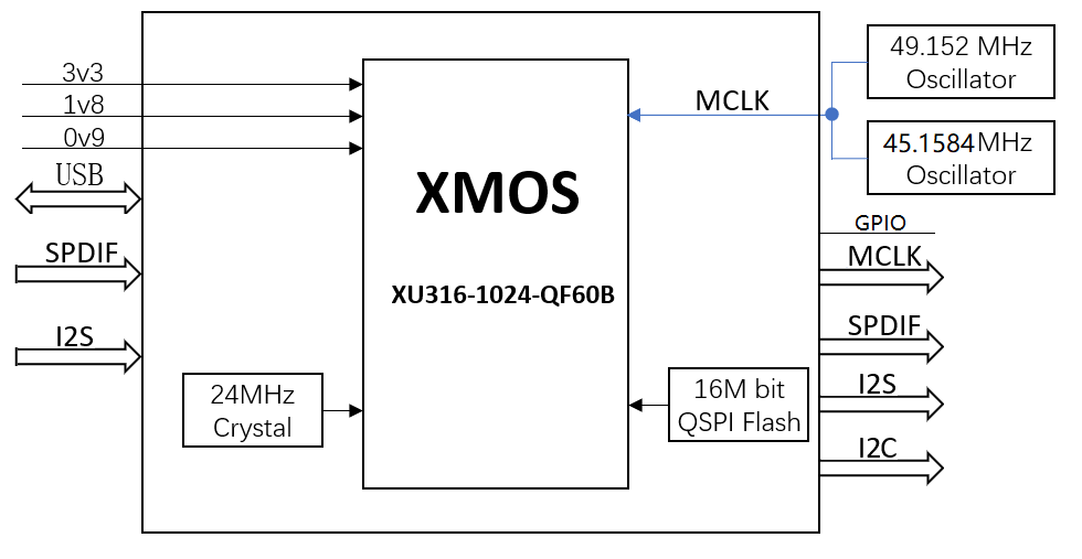
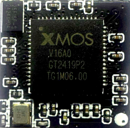
1. Product Introduction 1.1 Product Description A316-Mini-V1 is a Mini module designed for small-sized products with dimensions of only 13mm x 13mm, specifically designed for space-constrained high-end audio systems. The module integrates the XU316-1024-QF60BC24 chip and includes a built-in 24MHz crystal and 16Mbit Flash for firmware storage. With different firmware, A316-Mini-V1 can meet various audio application solution requirements. 1.2 Product Features Hardware Configuration 3.3V, 1.8V, 0.9V Power Supply Integrated 16Mbit QSPI Flash for firmware and data storage USB Interface Features USB 2.0 (Full-speed and High-speed) USB Audio Class 1.0 USB Audio Class 2.0 System Compatibility UAC 2.0 protocol, supports ASIO, compatible with multiple operating systems including Windows, Linux, Android, macOS and iOS 1.3 Product Block Diagram 1.4 Specification Description Specification Item Description Product Name A316-Mini-V1 Product Description Ultra-Compact XU316 Module Package Type SMT LGA Environmental Compliance All hardware components fully comply with EU RoHS Directive
1.5 Absolute Maximum Ratings Parameter Minimum Maximum Unit Storage Temperature -40 125 ℃ Supply Voltage -0.5 3.63 V 1.8V Supply Voltage -0.5 1.98 V 0.9V Supply Voltage -0.5 1.05 V ESD Voltage (Human Body Model) TAMB-25℃ -2 2 KV ESD Voltage (Machine Model) TAMB-25℃ -500 500 V
1.6 Normal Operating Conditions Function Minimum Typical Maximum Unit Operating Temperature 0 - 70 ℃ 3.3V Operating Voltage 3.0 3.3 3.6 V 1.8V Operating Voltage 1.62 1.80 1.98 V 0.9V Operating Voltage 0.855 0.90 0.945 V
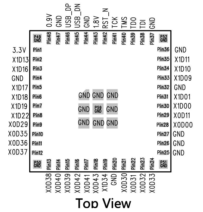
1.7 Operating Current 2. Pin Definition 2.1 Pin Layout Top View 2.2 Pin Description Module Pin Number Name Type Function 1 3.3V P Module 3.3V Power Supply 2 X1D13 I/O Multi-function GPIO 3 X1D16 I/O Multi-function GPIO 4 GND P Module Ground 5 X1D17 I/O Multi-function GPIO 6 X1D18 I/O Multi-function GPIO 7 X1D19 I/O Multi-function GPIO 8 X1D22 I/O Multi-function GPIO 9 X0D29 I/O Multi-function GPIO 10 X0D35 I/O Multi-function GPIO 11 X0D36 I/O Multi-function GPIO 12 X0D37 I/O Multi-function GPIO 13 X0D38 I/O Multi-function GPIO 14 X0D40 I/O Multi-function GPIO 15 X0D39 I/O Multi-function GPIO 16 X0D42 I/O Multi-function GPIO 17 X0D41 I/O Multi-function GPIO 18 X0D43 I/O Multi-function GPIO 19 X1D34 I/O Multi-function GPIO 20 GND P Module Ground 21 X0D30 I/O Multi-function GPIO 22 X0D31 I/O Multi-function GPIO 23 X0D32 I/O Multi-function GPIO 24 X0D33 I/O Multi-function GPIO 25 GND P Module Ground 26 GND P Module Ground 27 GND P Module Ground 28 X0D00 I/O Multi-function GPIO 29 X0D11 I/O Multi-function GPIO 30 X1D00 I/O Multi-function GPIO 31 X1D01 I/O Multi-function GPIO 32 GND P Module Ground 33 X1D09 I/O Multi-function GPIO 34 X1D10 I/O Multi-function GPIO 35 X1D11 I/O Multi-function GPIO/XU316 Internal Clock Output 36 GND P Module Ground 37 GND P Module Ground 38 TDI I/O Multi-function GPIO 39 TDO I/O Multi-function GPIO 40 TMS I/O Multi-function GPIO 41 TCK I/O Multi-function GPIO 42 RST_N I/O Multi-function GPIO 43 1.8V P Module 1.8V Power Supply 44 GND P Module Ground 45 USB_DM I/O USB_DM 46 USB_DP I/O USB_DP 47 GND P Module Ground 48 0.9V P Module 0.9V Power Supply 49 GND P Module Ground 50 GND P Module Ground 51 GND P Module Ground 52 GND P Module Ground
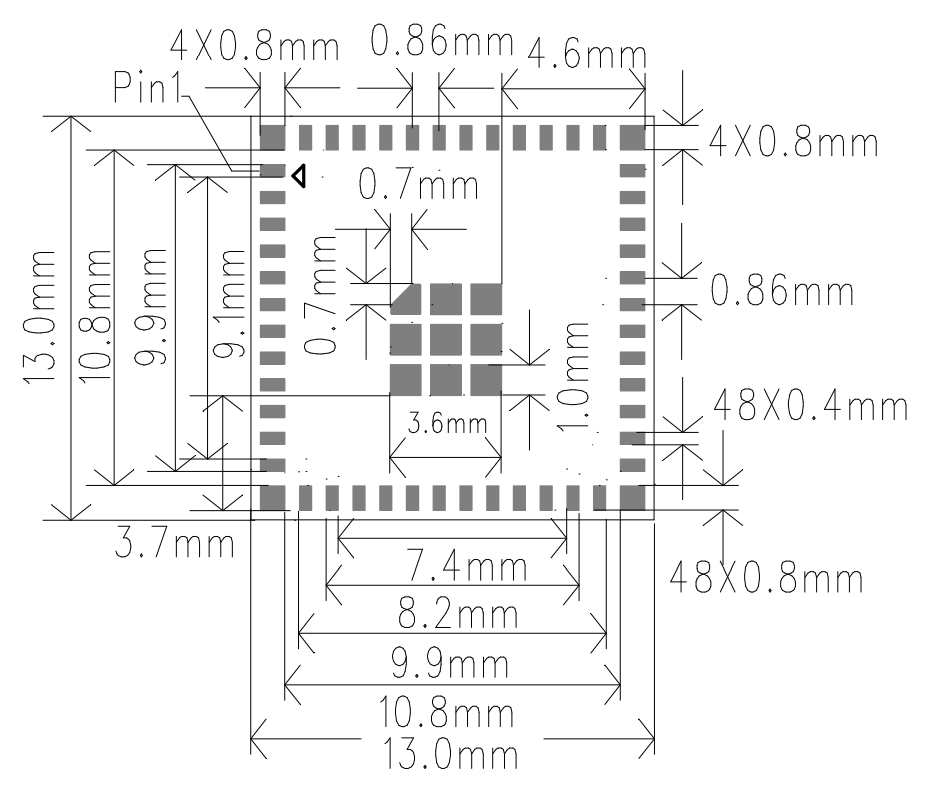
3.1 Module Dimensions PCB Dimensions:
13±0.1mm(L)X13±0.1mm(W)X0.8±0.1mm(H)
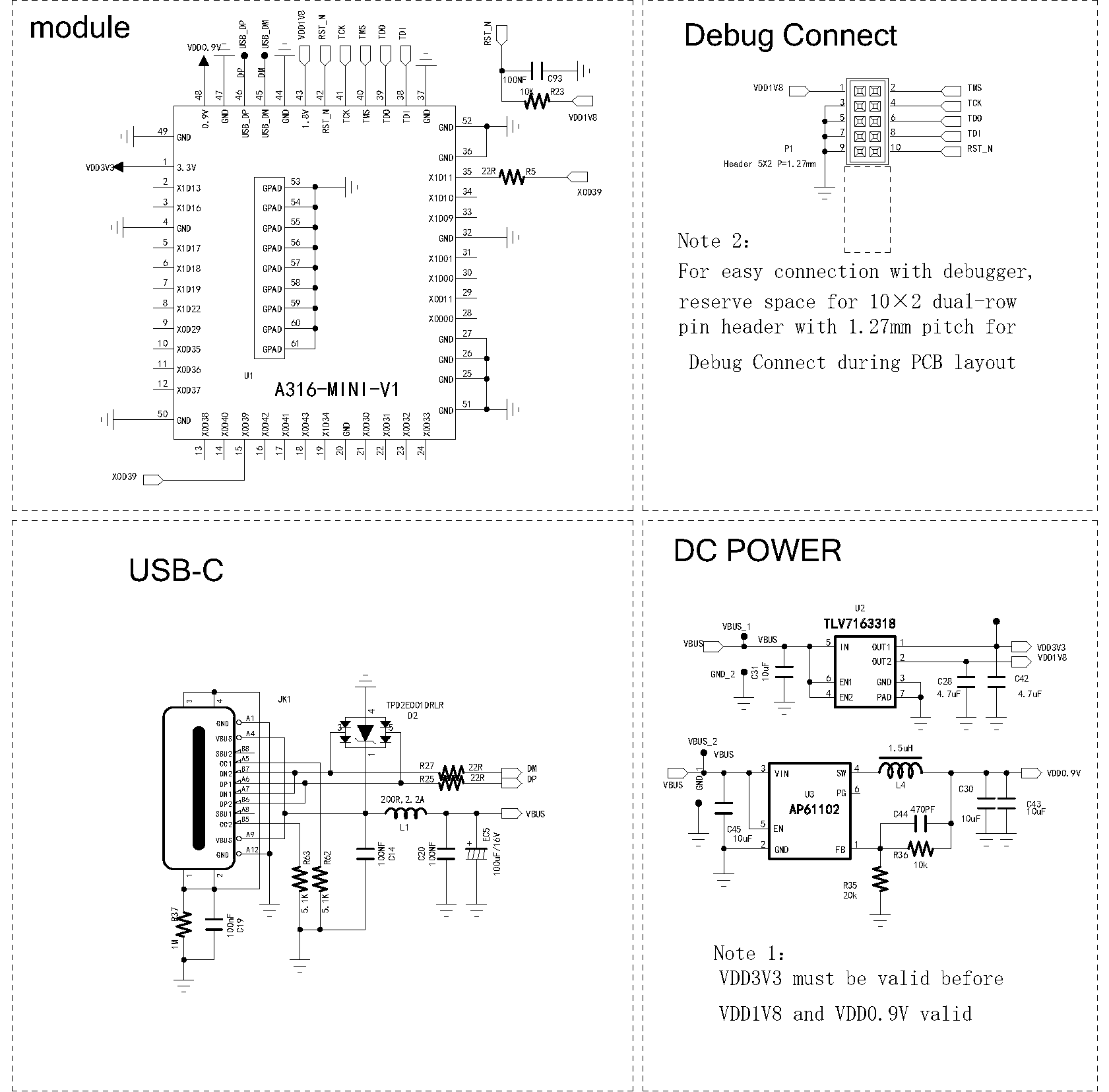
4. Minimum System Reference Design Tray + Outer Box Packaging
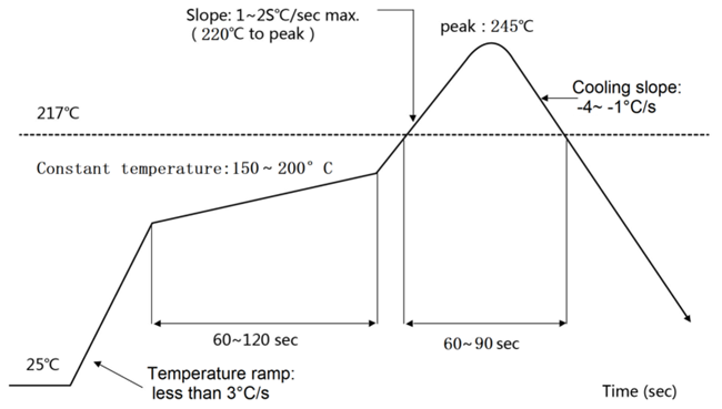
6. Recommended Reflow Soldering Temperature Profile 7. Revision History Version Date Description Revised by V1.0 2025-05-07 Initial Release V1.1 2025-10-07 Added minimum system reference design
8. Inquiry and Feedback Click to Expand Inquiry and Feedback Form 